- 您现在的位置:买卖IC网 > Sheet目录322 > DS24B33G+T&R (Maxim Integrated Products)IC EEPROM 4KBIT 2SFN
�� �
�
�DS24B33�
�1-Wire� 4Kb� EEPROM�
�Slave-to-Master�
�A� read-data� time� slot� begins� like� a� write-one� time� slot.�
�The� voltage� on� the� data� line� must� remain� below� V� TL�
�until� the� read� low� time� t� RL� is� expired.� During� the� t� RL� win-�
�dow,� when� responding� with� a� 0,� the� DS24B33� starts�
�pulling� the� data� line� low;� its� internal� timing� generator�
�determines� when� this� pulldown� ends� and� the� voltage�
�starts� rising� again.� When� responding� with� a� 1,� the�
�DS24B33� does� not� hold� the� data� line� low� at� all,� and� the�
�voltage� starts� rising� as� soon� as� t� RL� is� over.�
�The� sum� of� t� RL� +� δ� (rise� time)� on� one� side� and� the� inter-�
�nal� timing� generator� of� the� DS24B33� on� the� other� side�
�define� the� master� sampling� window� (t� MSRMIN� to�
�t� MSRMAX� )� in� which� the� master� must� perform� a� read� from�
�the� data� line.� For� the� most� reliable� communication,� t� RL�
�should� be� as� short� as� permissible,� and� the� master�
�should� read� close� to� but� no� later� than� t� MSRMAX� .� After�
�reading� from� the� data� line,� the� master� must� wait� until�
�t� SLOT� is� expired.� This� guarantees� sufficient� recovery�
�time� t� REC� for� the� DS24B33� to� get� ready� for� the� next� time�
�slot.� Note� that� t� REC� specified� herein� applies� only� to� a�
�single� DS24B33� attached� to� a� 1-Wire� line.� For� multide-�
�vice� configurations,� t� REC� needs� to� be� extended� to�
�accommodate� the� additional� 1-Wire� device� input�
�capacitance.� Alternatively,� an� interface� that� performs�
�active� pullup� during� the� 1-Wire� recovery� time� such� as�
�the� DS2482-x00� or� DS2480B� 1-Wire� line� drivers� can� be�
�used.�
�Improved� Network� Behavior�
�(Switchpoint� Hysteresis)�
�In� a� 1-Wire� environment,� line� termination� is� possible�
�only� during� transients� controlled� by� the� bus� master�
�(1-Wire� driver).� 1-Wire� networks,� therefore,� are� suscep-�
�tible� to� noise� of� various� origins.� Depending� on� the� phys-�
�ical� size� and� topology� of� the� network,� reflections� from�
�end� points� and� branch� points� can� add� up� or� cancel�
�each� other� to� some� extent.� Such� reflections� are� visible�
�as� glitches� or� ringing� on� the� 1-Wire� communication� line.�
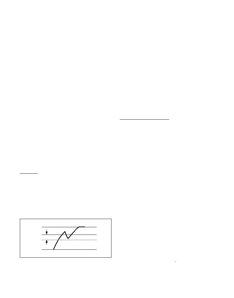
�V� PUP�
�Noise� coupled� onto� the� 1-Wire� line� from� external�
�sources� can� also� result� in� signal� glitching.� A� glitch� dur-�
�ing� the� rising� edge� of� a� time� slot� can� cause� a� slave�
�device� to� lose� synchronization� with� the� master� and,�
�consequently,� result� in� a� Search� ROM� command� com-�
�ing� to� a� dead� end� or� cause� a� device-specific� function�
�command� to� abort.� For� better� performance� in� network�
�applications,� the� DS24B33� uses� an� improved� 1-Wire�
�front-end,� which� makes� it� less� sensitive� to� noise.�
�The� 1-Wire� front-end� of� the� DS24B33� differs� from� tradi-�
�tional� slave� devices� in� one� characteristic:� There� is� a� hys-�
�teresis� at� the� low-to-high� switching� threshold� V� TH� .� If� a�
�negative� glitch� crosses� V� TH� but� does� not� go� below�
�V� TH� -� V� HY� ,� it� is� not� recognized� (Figure� 12).� The� hysteresis�
�is� effective� at� any� 1-Wire� speed.�
�CRC� Generation�
�The� DS24B33� uses� two� different� types� of� CRCs.� One�
�CRC� is� an� 8-bit� type� and� is� stored� in� the� most� signifi-�
�cant� byte� of� the� 64-bit� registration� number.� The� bus�
�master� can� compute� a� CRC� value� from� the� first� 56� bits�
�of� the� 64-bit� registration� number� and� compare� it� to� the�
�value� stored� within� the� DS24B33� to� determine� if� the� reg-�
�istration� number� has� been� received� error-free.� The�
�equivalent� polynomial� function� of� this� CRC� is� X� 8� +� X� 5� +�
�X� 4� +� 1.� This� 8-bit� CRC� is� received� in� the� true� (noninvert-�
�ed)� form.� It� is� computed� and� programmed� into� the� chip�
�at� the� factory.�
�The� other� CRC� is� a� 16-bit� type,� generated� according� to�
�the� standardized� CRC-16� polynomial� function� X� 16� +� X� 15�
�+� X� 2� +� 1.� This� CRC� is� used� for� fast� verification� of� a� data�
�transfer� when� writing� to� the� scratchpad.� In� contrast� to�
�the� 8-bit� CRC,� the� 16-bit� CRC� is� always� communicated�
�in� the� inverted� form.� A� CRC� generator� inside� the�
�DS24B33� (Figure� 13)� calculates� a� new� 16-bit� CRC,� as�
�shown� in� the� command� flowchart� (Figure� 7).� The� bus�
�master� compares� the� CRC� value� read� from� the� device�
�to� the� one� it� calculates� from� the� data,� and� decides�
�whether� to� continue� with� an� operation.�
�With� the� Write� Scratchpad� command,� the� CRC� is� gen-�
�erated� by� first� clearing� the� CRC� generator� and� then�
�shifting� in� the� command� code,� the� target� addresses�
�TA1� and� TA2,� and� all� the� data� bytes� as� they� were� sent�
�V� TH�
�0V�
�V� HY�
�by� the� bus� master.� The� DS24B33� transmits� this� CRC�
�only� if� the� data� bytes� written� to� the� scratchpad� include�
�scratchpad� ending� offset� 11111b.� The� data� can� start� at�
�any� location� within� the� scratchpad.�
�For� more� information� on� generating� CRC� values� refer� to�
�Application� Note� 27:� Understanding� and� Using� Cyclic�
�Figure� 12.� Hysteresis� at� the� Low-to-High� Switching� Threshold�
�Maxim� Integrated�
�Redundancy� Checks� with� Maxim� iButton� Products.�
�19�
�发布紧急采购,3分钟左右您将得到回复。
相关PDF资料
DS2502-E64+
IC OTP 1KBIT TO92-3
DS2502P-E48+T&R
IC OTP 1KBIT 6TSOC
DS2502S+
IC OTP 1KBIT 8SOIC
DS2505+T&R
IC OTP 16KBIT TO92-3
DS25LV02R+T&R
IC OTP 1KBIT SOT23-5
DS2704G+T&R
IC EEPROM 1.25KBIT 6TDFN
DS28CZ04G-4+T
IC EEPROM 4KBIT 400KHZ 12TQFN
DS28DG02E-3C+T
IC EEPROM 2KBIT 2MHZ 28TSSOP
相关代理商/技术参数
DS24B33G+U
功能描述:电可擦除可编程只读存储器 1-WIRE 4KB 电可擦除可编程只读存储器 RoHS:否 制造商:Atmel 存储容量:2 Kbit 组织:256 B x 8 数据保留:100 yr 最大时钟频率:1000 KHz 最大工作电流:6 uA 工作电源电压:1.7 V to 5.5 V 最大工作温度:+ 85 C 安装风格:SMD/SMT 封装 / 箱体:SOIC-8
DS24B33Q+T&R
制造商:Maxim Integrated Products 功能描述:1-WIRE 4KB EEPROM - Tape and Reel 制造商:Maxim Integrated Products 功能描述:IC EEPROM 4KBIT 6TDFN 制造商:Maxim Integrated Products 功能描述:EEPROM 1-Wire 4kbit EEPROM
DS24B33Q+T&R
功能描述:电可擦除可编程只读存储器 1-Wire 4kbit 电可擦除可编程只读存储器 RoHS:否 制造商:Atmel 存储容量:2 Kbit 组织:256 B x 8 数据保留:100 yr 最大时钟频率:1000 KHz 最大工作电流:6 uA 工作电源电压:1.7 V to 5.5 V 最大工作温度:+ 85 C 安装风格:SMD/SMT 封装 / 箱体:SOIC-8
DS24B33Q+U
功能描述:电可擦除可编程只读存储器 1-WIRE 4KB 电可擦除可编程只读存储器 RoHS:否 制造商:Atmel 存储容量:2 Kbit 组织:256 B x 8 数据保留:100 yr 最大时钟频率:1000 KHz 最大工作电流:6 uA 工作电源电压:1.7 V to 5.5 V 最大工作温度:+ 85 C 安装风格:SMD/SMT 封装 / 箱体:SOIC-8
DS24B33S
制造商:MAXIM 制造商全称:Maxim Integrated Products 功能描述:1-Wire 4Kb EEPROM
DS24B33S R
制造商:MAXIM 制造商全称:Maxim Integrated Products 功能描述:1-Wire 4Kb EEPROM
DS24B33S T
制造商:MAXIM 制造商全称:Maxim Integrated Products 功能描述:1-Wire 4Kb EEPROM
DS24B33S TR
制造商:MAXIM 制造商全称:Maxim Integrated Products 功能描述:1-Wire 4Kb EEPROM